Size-dependent Properties of Nanostructures
Nanotechnology is the key enabling technology for development of revolutionary devices in communications, biotechnology, and storage/processing of digital information. This diverse range of applications benefits from the unique ability of nanostructures to control the material properties: electronic, optical, and magnetic.


In other words, engineers designing nanoscale devices are not bound by the bulk properties of traditional materials, but rather can customize the characteristics of nanostructures by controlling their size and shape.
For example, as the size of quantum dots changes, so does the color of their fluorescence, even though the "parent" material stays the same. By contrast, in a macroscopic system changing the material is essentially the only way to change the color of the fluorescence across a similarly broad spectrum. Furthermore, new properties can emerge in nanoscale materials. For example, silicon, which in bulk does not emit light, can become fluorescent in nanostructures, because quantum confinement induces changes in the electronic structure (band structure) of silicon.
Electrons in Nanostructures
Transport and confinement of electrons in a material determine most of the electronic, optical, and magnetic properties. The appropriate sizes of nanostructures can then be estimated by considering the effect of confinement inside a small structure on a single electron with mass m and charge e. The corresponding energy scale is determined by the required operating temperature. Most practical devices have to operate close to room temperature, i.e., the scale of thermal fluctuations kT is around 25 meV.
The following model systems are based on different physical effects: quantum confinement, electrostatics, and magnetism. Nevertheless, in all three cases new properties emerge at essentially the same nanoscale: 1–10 nm.
Quantum Confinement

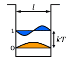
The simplest way to model the effect of quantum confinement on the energy of an electron is to consider it as a "particle-in-a-box" problem. For an electron inside a potential well of width l, the spacing between the lowest two quantum energy levels is:

If we require EQM > 25 meV to prevent thermal excitations, the width of the well must be l < 7 nm.
Single-electron Electrostatics

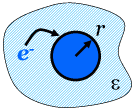
For a single electron on a sphere of radius r surrounded by a medium with dielectric constant ε, the Coulomb energy is:

Using ε of silicon and imposing the EC > 25 meV requirement, we obtain an upper limit for the diameter of that sphere (nanoparticle) of 2r < 9 nm.
The Superparamagnetic Limit

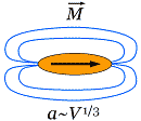
Macroscopic magnetic particles typically contain a number of magnetization domains, each, in principle, with magnetization along a different direction. As particles become smaller, the number of separate magnetic domains decreases until there is only one left—the entire particle. The minimum size of a particle used in magnetic data storage is determined from the requirement that its magnetization M cannot be randomly "flipped" by thermal fluctuations.
Such particles are called superparamagnetic, and the corresponding size limit a is known as the superparamagnetic limit. A quantitative estimate of a depends on the specific recording and readout scheme, but a typical value for many practical recording media is a ~ 3–5 nm.
References
- Tutorial on nanoscience and nanotechnology by F.J. Himpsel.
- Self-Assembled Nanostructures at Silicon Surfaces (2.2 MB)
by D.Y. Petrovykh and F.J. Himpsel for the Encyclopedia of Nanoscience and Nanotechnology.