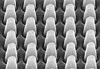
Size-uniformity and Ordering of Nanostructures
Nanostructures with dimensions below 10 nm hold the most potential for new science, devices, and applications. At the same time, even with the impressive advances in conventional photolithography and other techniques for sub-100-nm fabrication, the inherent limitations of the top-down design and manufacturing become difficult to negotiate at the sub-10-nm scale, i.e., exactly at the scale where material properties become size-dependent.

Furthermore, ordered arrangements of size-controlled nanostructures are usually required for device applications. For example, in single-electron transistors or in quantum computing qubits, interactions between the nanostructures need to be precisely controlled and registration with the next level of the device (or external contacts) has to be maintained. On the other hand, for optical and electronics applications that do not require quantum coherence, the high packing density and size uniformity of nanostructures become more significant than their ordering. For the ultimate storage media both high density and precise positioning over macroscopic areas are desired.
Self-assembly vs. Self-organization
In self-assembly, interactions between atoms, nanostructures, and their environment produce kinetically or thermodynamically preferred structures and patterns. Self-assembly is inherently parallel and thus is able to produce macroscopic amounts of nanostructures. There are two types of spontaneous processes important for creating nanostructures: self-assembly and self-organization.
- Self-assembly of nanostructures can be defined as the spontaneous formation of structures smaller than 10 nm (in at least one dimension) and with a well-defined size distribution.
- Self-organization in nanoscale systems involves their natural tendency to form structures with long-range order, i.e., order at the scale much larger than the size of an individual nanostructure.
In general, self-assembly is required to produce large numbers of individual nanoparticles (or nanostructures) having unique and/or tailored properties. Self-organization provides a pathway for combining nanostructures into novel materials or for establishing connections between nanostructures and the macroscopic world.
Self-assembly and self-organization need not coexist in the same system, i.e., self-assembled nanostructures do not always self-organize and self-organization is not exclusive to self-assembled nanostructures. But for practical nanotechnology, systems that exhibit both self-assembly and self-organization are desirable.
Self-assembled Monolayers
No discussion of self-assembly would be complete without a mention of self-assembled monolayers (SAMs)—the films of (organic) molecules that spontaneously form on solid or liquid surfaces and typically possess some degree of long-range (crystalline) order. One might argue that "self-organized" monolayers would have been a more accurate description of a prototypical SAM, but historically the term "self-assembled" is universally used. The resulting ambiguity is in part responsible for a debate within the research community: should the term be applied only to monolayers that are formed near the thermodynamic equilibrium for a given system, or can we also call "SAMs" monolayers that form via a predominantly kinetic process (e.g., via irreversible surface adsorption)?
Inorganic Self-assembly
In contrast to the above SAM debate, many inorganic surface systems, such as quantum dots on semiconductors, are known to be thermodynamically unstable, but nevertheless are universally referred to as "self-assembled" structures. In absence of universally-accepted definitions, it is therefore advisable to indicate specific system properties on a case-by-case basis, rather than assume that describing a system as "self-assembled" is sufficiently self-explanatory (no pun intended).
Surfaces and Self-assembly
Surfaces offer many advantages as platforms for self-assembly and self-organization of nanostructures. The majority of current techniques for fabrication and characterization of nanostructures are surface-based. Even 3D structures created by lithography or molecular beam epitaxy (MBE) are actually stacks of multiple layers, hence the surface processes on the topmost layer play the key role during growth.
Numerous applications in microelectronics and wide availability of high-quality single-crystal substrates made semiconductor surfaces—especially those of silicon and III-V semiconductors—the most studied and the best understood surface systems. In particular, methods for preparing, cleaning, analyzing, and modifying semiconductor surfaces are well developed and most of them can be adapted for nanoscience.
Surfaces are also characterized by multiple scales of physical processes and interactions—a property extremely important for achieving directed self-assembly and self-organization. Different parameters during the growth and post-processing of nanostructures can be independently controlled in order to selectively enable the particular mechanism(s) at appropriate stages. Atomistic processes ultimately define the dynamics and thermodynamics of nanostructures and thus their self-assembly on surfaces. On a slightly larger scale, surface stress is a factor important for both self-assembly and self-organization. Surface defects, in particular atomic steps, extend self-organization up to macroscopic scales. Selecting an individual dominant mechanism or enabling an interplay between several processes is often as simple as changing the temperature of the surface.
Overall, surfaces provide a well-controlled, well-characterized, and versatile environment for practical nanoscience and nanotechnology. Specific examples and illustrations of the basic principles discussed above are only briefly presented in this introduction to nanoscience, but details are available from the following references.
References
- Self-Assembled Nanostructures at Silicon Surfaces (2.2 MB)
by D.Y. Petrovykh and F.J. Himpsel for the Encyclopedia of Nanoscience and Nanotechnology. - Self-Assembly of One-Dimensional Nanostructures at Silicon Surfaces (950 kB)
Solid State Commun. 117, 149 (2001). - Self-Organization of Nanostructures in Semiconductor Heteroepitaxy, review by C. Teichert
Phys. Rep. 365, 335 (2002). DOI: 10.1016/S0370-1573(02)00009-1 - Self-Assembled Monolayers of Alkanethiols on InAs (1.3 MB),
Langmuir, 25, 12185 (2009). - Alkanethiols on Platinum: Multicomponent Self-Assembled Monolayers (405 kB),
Langmuir 22, 2578 (2006).