Types of Nanoscale Templates
Anyone who has used a muffin tin or an egg carton knows the basic concepts of using a template to form and to arrange objects. In the nanoworld, the templates just need to be designed for much smaller objects—nanostructures.
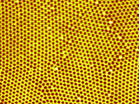
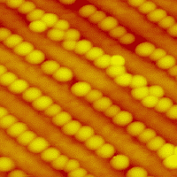
Ordered arrays of hexagonally-packed nanopores can be formed by electrochemical oxidation of thin aluminum membranes. These pores can subsequently be filled (also electrochemically) by other materials (metals and/or polymers) to form a large number of nearly-identical nanowires.
Patterns with features as small as 10–100 nm can be stamped and then cured in poly(dimethylsiloxane) (PDMS) films. Nanoparticles deposited on such templates from solution are driven by differences in surface chemistry and wettability, which often leads to self-organization along the template features.
These two examples illustrate the two general types of templates: self-assembled and patterned. Self-assembled templates (which are typically also self-organized) are created via spontaneous nanostructuring of a substrate material under controlled external conditions: temperature, electrochemical reactions, deposition or evaporation of material, etc. This approach potentially can be scaled up to produce enough high-quality templates for manufacturing purposes. The caveat is that currently only rather simple, usually highly-symmetric, ordering is routinely achievable by this method. More complex templates still require some form of patterning, e.g., replicating a master stamp, defining features by lithography, or using bio-inspired templates.
Self-organized Templates on Silicon Surfaces
Atomic steps always form on macroscopic surfaces, so self-organization schemes can naturally benefit from the presence of steps, rather than attempt to eliminate them. For example, step-flow growth techniques, used in microelectronics industry, take advantage of surface steps for initiating smooth growth of semiconductor films.
To produce surface steps with controlled density and orientation, a silicon wafer can be intentionally miscut by a small angle (α < 1–10°) away from a stable atomically-flat surface, such as {111} or {001}. Energetically, the resulting vicinal surface prefers to maintain the parent low-index orientation, but it is forced to comply with the overall miscut angle, which is accomplished by introducing atomic steps separated by flat terraces (of the parent low-index orientation).
The average width of the terraces and the number of steps separating them are determined by the miscut angle α. For α < 1–2°, steps predominantly form with a height of a few atomic layers, producing "atomic staircases".
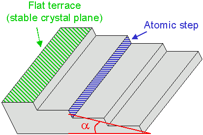
An atomic staircase consists of flat low-index terraces (shaded green) separated by atomic steps (shaded blue). On Si(111) such stepped surfaces only form for miscut angles α < 1–2°.
At larger miscut angles, step bunches can combine to form a second stable (high-index) facet, producing a surface with two alternating facets, which looks like an "atomic washboard".
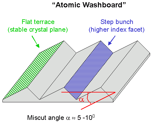
An "atomic washboard" forms for miscut angles α of 5–10° and consists of alternating stable low- and high-index facets.
Dynamics of steps on the vicinal surface can be controlled by macroscopic parameters: miscut angle, temperature, deposition and annealing rate, etc. Self-organized arrays of steps (or step bunches) represent surface templates macroscopic in one direction (along the steps) and nanoscale in two other directions (step separations and heights).
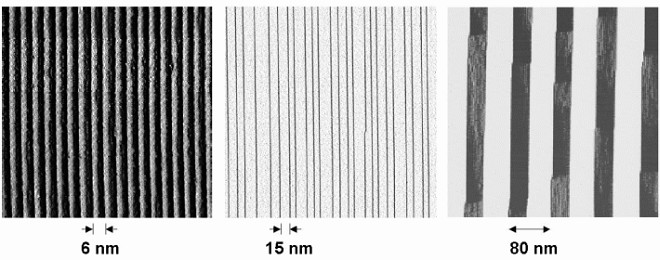
Self-organized nanoscale templates on vicinal silicon surfaces. The derivative of the STM topography is shown on these images in order to highlight the atomic steps, which appear as vertical dark lines. In other words, in this representation the surfaces appear to be illuminated from the left.
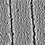
Particularly straight atomic steps can be prepared on vicinal Si(111) surfaces. The unique stability and large unit cell of the Si(111)7×7 surface reconstruction effectively forces the silicon atomic steps to follow a specific high-symmetry direction on the Si(111) surface. Arrays of atomic steps with as few as 1 kink in 20,000 atomic sites have been prepared by the group of Franz Himpsel.
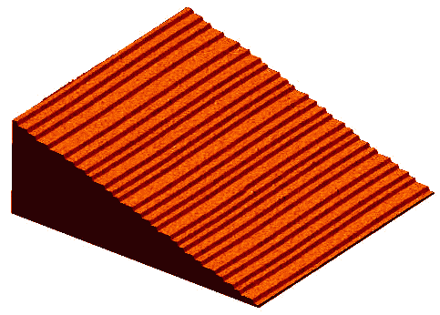
3D view of an STM image of a stepped Si(111) surface. Each step of this atomic staircase is ~0.3 nm high. The miscut angle for this surface is ~1°, so the vertical axis is stretched by a factor of 15 to clearly show the steps.
Those templates held the record for uniformity of atomic steps, until almost 10 years later the procedure was improved by the Itoh group, who produced steps with nearly-perfect atomic structure over several μm2.
Patterned Surface Templates
Template-based self-organization is certainly going to be important for practical devices. For example, the output of solid-state electronics is based on macroscopic circuitry, and thus connections and alignment between the nanoscale elements and the appropriate "leads" must be provided; similar "bridging" of the gap in scales is needed in many other applications.
To obtain arbitrary and complex patterns, the self-organization driven by properties of individual self-assembled particles may be aided by the top-to-bottom "instructions" provided by the template. The alternative view of such a process is that of a template as a basis for the bottom-up assembly of simple structural elements, e.g., by ensuring appropriate anchoring of components for molecular electronics. Thus, in general, introducing templates to aid self-assembly and self-organization allows one to combine beneficial characteristics of the bottom-up and top-to-bottom approaches.
The simplest way to prepare a surface template is to define the desired pattern using one's method of choice and then to selectively add (or subtract) material(s) to form the structures. The deposited material may also be in form of pre-assembled nanostructures, e.g., nanoparticles. Strictly speaking, deposition onto a pre-patterned surface involves only rudimentary self-organization—via direct selectivity of the deposition process to the pre-defined pattern. The caveat of the direct patterning approach is that the chosen method must be capable to produce structures at the required resolution. The complexity (but generally not the surface density) of the patterned structures can be increased by post-processing, e.g., etching or heating.
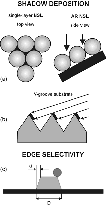
Size reduction methods can extend the patterning resolution; two most common methods of size reduction are shadow deposition and edge selectivity. Both these methods take advantage of geometric factors. Specifically, gaps or overlaps between "shadowed" regions can be smaller than the structures casting the shadows. Similarly, edges of any structure are geometrically smaller than the structure itself, hence edge selective processes can effectively enhance resolution of a pattern.
References
- Self-Assembled Nanostructures at Silicon Surfaces (2.2 MB)
by D.Y. Petrovykh and F.J. Himpsel for the Encyclopedia of Nanoscience and Nanotechnology. - Regular Step Arrays on Silicon (620 kB), Appl. Phys. Lett. 72, 948 (1998).
- Formation of Regular Step Arrays on Si(111)7×7 (990 kB), J. Appl. Phys. 84, 255 (1998).
- Atomically Accurate Si Grating with 5.73 nm Period (360 kB), Appl. Phys. Lett. 79, 1608 (2001).
- Atomically Straight Steps on Vicinal Si(111) Surfaces Prepared by Step-parallel Current in the Kink-up Direction, Appl. Phys. Lett. 87, 031903 (2005). DOI: 10.1063/1.1995946
- Self-Organization of Nanostructures in Semiconductor Heteroepitaxy, review by C. Teichert
Phys. Rep. 365, 335 (2002). DOI: 10.1016/S0370-1573(02)00009-1