Self-assembled Nanostructures by Step-decoration
Self-assembled nanostructures shown below were created using the step-decoration technique. The technique is as old as surface science—atomic planes and steps on crystal surfaces of alkali-halides have been first visualized by decoration with gold. Nanoscale step decoration is not visible in an optical micrograph, but the principle is the same. Evaporate some foreign material onto a clean crystal surface, and if the temperature of the surface is sufficiently high, the deposited atoms will diffuse towards and accumulate along the surface steps. The real-world analogy is throwing some marbles onto a washboard and shaking the washboard to evenly redistribute the marbles between the grooves.
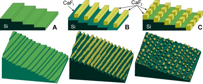
Self-assembly by step-decoration of vicinal Si(111) templates. The schematic diagram (top) and 3D representation of the STM data (bottom) are color-coded to indicate the silicon substrate (green) and CaF2 nanostructures (yellow).
(A) "Atomic staircase" on a vicinal Si(111) surface used as the nanoscale template for structures in (B) and (C).
(B) Self-assembled CaF2 nanostripes on upper edges of the silicon steps.
(C) Self-assembled CaF2 nanodots at lower edges of the silicon steps.
Molecular Nanowires
The CaF2 stripes shown above are not "wires" in a conventional sense, because they will not conduct any current—CaF2 is actually an excellent insulator. But these arrays of CaF2 nanostripes separated by CaF1 trenches can themselves serve as nanoscale templates. It turns out that for some organic molecules the chemical interactions and diffusion coefficients differ significantly between CaF2 and CaF1, enough to effectively confine the molecules along the CaF1 trenches.
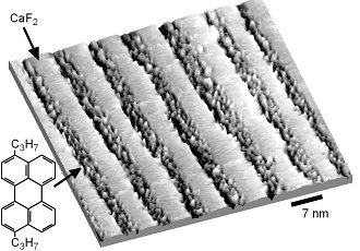
Quasi one-dimensional confinement of organic molecules. Molecules of 3,10-di(propyl)perylene (DPP) selectively adsorb between CaF2 nanostripes on a self-organized CaF2/CaF1 template. By adjusting the width of the CaF2 stripes, the molecules can be confined along trenches as narrow as 3-4 nm.
Molecules confined in this quasi one-dimensional geometry offer an opportunity for forming either molecular wires or metallic nanowires. For the former, the molecules themselves need to be conducting and overlapping along the trench to form a continuous molecular wire. For the latter, the molecules are rather used as precursors that are subsequently converted into a metal wire.
Growth Modes on Flat Surfaces
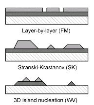
In the thermodynamic limit, the roughness of a film growing on a flat surface is determined by the relative free surface energies γ of the substrate, the adsorbate (film), and the interface.
In the layer-by-layer (Frank-van der Merwe or FM) mode a low surface energy adsorbate wets the substrate with a continuous film and higher layers do not start growing until the topmost one is nearly complete.
γsubstrate > γadsorbate + γinterface
In Stranski-Krastanov (SK) mode, the first adsorbate layer reduces the substrate surface energy enough to stop the wetting behavior, and the growth continues as 3D islands.
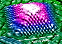
Finally, for an adsorbate having high surface energy, random disjointed 3D islands form, leaving most of the substrate exposed (Volmer-Weber or VW mode).
γsubstrate < γadsorbate + γinterface
Two of these three equilibrium growth modes (SK and VW) can produce self-assembled nanodots, Ge pyramids on Si surfaces being, perhaps, the most famous example. Self-organization in such systems is typically limited to nearest-neighbor interactions, but can become significant in multilayer systems.
The three equilibrium growth modes, however, depend on two important assumptions that often are not satisfied. First, the assumption of lattice-matched materials is in general not true, in particular in cases of technologically relevant material combinations (e.g., Ge/Si). Second, the assumption of an equilibrium process is not always satisfied even approximately (and never exactly, since all experiments are of finite duration).
2D Growth Modes on Stepped Surfaces
Growth of nanostructures on stepped (vicinal) surfaces is actually more complicated than the simple step decoration idea may suggest. In fact, all the equilibrium 3D growth modes can be generalized for 2D growth on stepped surfaces by replacing the surface free energies γ with the respective step energies σ. A new, uniquely 2D equilibrium growth mode is described mathematically as:
σinterface > σadsorbate + σsubstrate
In this case adsorbate islands avoid (or are effectively "repelled" by) the steps, which is a uniquely 2D possibility, as in the 3D equivalent the islands would have to be floating above the surface.
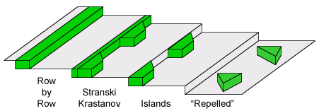
2D equilibrium growth modes at steps.
Non-equilibrium growth in 2D occurs at temperatures lower and growth rates higher than those required for quasi-equilibrium. Specifically, diffusion is suppressed as the temperature is reduced: first diffusion across steps, then diffusion along step edges, and finally diffusion across terraces. For a system that exhibits row-by-row equilibrium growth the whole progression can be followed experimentally.
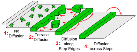
2D non-equilibrium growth modes at steps.
References
- Self-Assembled Nanostructures at Silicon Surfaces (2.2 MB)
by D.Y. Petrovykh and F.J. Himpsel for the Encyclopedia of Nanoscience and Nanotechnology. - Self-Assembly of One-Dimensional Nanostructures at Silicon Surfaces (950 kB)
Solid State Commun. 117, 149 (2001). - Linear Arrays of CaF2 Nanostructures on Si (520 kB), Appl. Phys. Lett. 74, 2125 (1999).
- One-Dimensional Confinement of Organic Molecules via Selective Adsorption on CaF1 vs. CaF2 (700 kB),
Chem. Phys. Lett. 303, 363 (1999). - Self-Assembled Fe Nanowires Using Organometallic CVD and CaF2 Masks on Stepped Si(111) (325 kB),
Appl. Phys. Lett. 78, 829 (2001). - Creation of 'Quantum Platelets' via Strain-Controlled Self-Organization at Steps (260 kB),
Phys. Rev. Lett. 85, 5380 (2000).