Diamond Lattice Structure
Silicon crystals have the diamond lattice structure where each atom forms four identical covalent bonds with its neighbours, resulting in a tetrahedral arrangement. A {111} plane is shown in the following schematic as the red triangle cutting diagonally across the cube. There are many {111} planes in each silicon crystal—all atomic planes parallel to the one highlighted in the figure are also {111} planes.
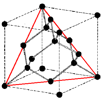
Schematic model of the diamond lattice structure. Note that each atom has four identical bonds to its neighbours. This tetrahedral arrangement of atoms is characteristic of the structure of diamond crystals, hence the "diamond lattice structure" designation. The red triangle highlights one of the {111} crystal planes.
Si(111) Surface
The Si(111) surface is a special {111} plane—the one that terminates a crystal. The "cork-ball" models below show the atomic arrangement for a (111) surface of a diamond-lattice crystal. This idealized, or bulk-terminated, structure assumes that surface atoms remain in the same positions that they would have occupied in a bulk material. These structure models show atoms color-coded according to their position: orange for the surface layer and green for the deeper layers.
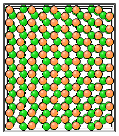
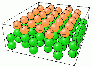
Cork-ball atomic models of an ideal (111) surface. The top view (left) clearly shows the three-fold symmetry of a (111) surface. The 3D view (right) demonstrates that in an ideal bulk-terminated (ideal) structure, the positions of the surface atoms (orange) relative to their neighbours are the same as for the atoms in the bulk layers (green).
Surface Explorer web-based tool was used to generate these models.
Surface Reconstruction
When a crystal is cut or cleaved to create a surface, most of the surface atoms lose bonding partners and are left with broken or dangling bonds. Such a configuration is energetically unfavorable and usually becomes unstable if the surface is heated up to a high enough temperature to allow the atoms to move. Upon heating under the ultra-high vacuum conditions, surface atoms rearrange into a configuration where some of the broken bonds can re-form; this new atomic arrangement is called a surface reconstruction.
Si(111)7×7 Surface Reconstruction
For clean Si(111) surfaces, a particularly stable reconstruction is the Si(111)7×7, with a diamond-shaped unit cell 7 atomic spacings on each side.
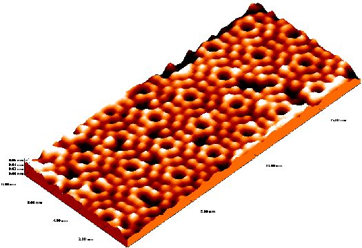
Atomic-resolution STM image of the Si(111)7×7 reconstruction. The 3D view uses the false-color height scale (sometimes called the temperature scale) in which brighter colors indicate higher features. The positions and sizes of protrusions on this STM image are close to the actual atomic arrangement on the Si(111)7×7 surface.
The image is 18×8 nm2, and the 0.04 nm height of the "bumps" is only a fraction of the Si atom size.
The Si(111)7×7 reconstruction has been appreciated by surface scientists for its beauty and complexity ever since Binnig and Rohrer produced their first 7×7 images shortly after they have invented the STM.
From the 1986 Nobel lecture by Binnig and Rohrer.
A most intriguing and challenging surface-science problem existed, namely, the 7×7 reconstruction of the Si(111) surface ... So we started to chase after the 7×7 structure, and succumbed to its magic.
We started the second 7×7 attempt in autumn 1982 taking into consideration the advice of Franz Himpsel not to sputter the surface. This immediately worked and we observed the 7×7 wherever the surface was flat. We were absolutely enchanted by the beauty of the pattern.
Dimer-Adatom-Stacking fault Model of Si(111)7×7
The only reliable method of assigning features in STM images is comparison with a surface structure model, such as the famous Dimer-Adatom-Stacking fault (DAS) model by Prof. Takayanagi. Color-coding in the fllowing figure refers to the different types of silicon atoms from the top three atomic layers that are involved in forming the 7×7 reconstruction. The DAS model indicates that the most prominent features in STM images correspond to the adatoms (yellow in the DAS model schematic).
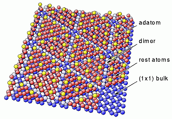
DAS model of the Si(111)7×7 (Takayanagi/Tong). Image from WWW picture gallery based on the Surface Structure Database (SSD, NIST Standard Reference Database 42) by P. R. Watson, M. A. Van Hove, K. Hermann. The picture has been prepared from SSD output and postprocessed with BALSAC by K. Hermann.
The DAS model also clearly shows corner-holes, i.e., areas at the corners of the 7×7 unit cells where atoms from the top three layers are missing. Corner-holes appear in STM images as dark areas surrounded by hexagons of adatoms or, on a larger scale, by six triangles, each triangle, in turn, composed of six adatoms.
Atomic Lego®
Structural elements of Si(111)7×7 can be highlighted by changing the sample bias during the STM imaging, as shown in the two examples below. Imaging at -1 V bias enhances the brightness of the dimer rows, resulting in the lattice-pie like appearance. By contrast, at -2 V bias, the dimer rows appear dark, but the two triangular halves of the Si(111)7×7 unit cell are highlighted. These two halves of the 7×7 unit cell are known as faulted and unfaulted in the DAS model, because the faulted half contains a stacking fault in the atomic layers.


Enhancing different features of the Si(111)7×7 reconstruction by adjusting the bias voltage. Two consecutive scans of an approximately 50×12 nm2 area on the sample at -1 V (left) and -2 V (right) sample bias.
The regularly-arranged holes and grids of parallel lines seen in the above images are reminiscent of Lego® baseboards (with a triangular rather than a square base unit). The Lego® analogy is instructive, because all of the structural elements of a Si(111)7×7 surface play an important part in guiding the self-assembly of nanostructures and atomic structures on these surfaces. For example, the lattice-work of lines seen in these STM images determines the positions of stable atomic steps on vicinal Si(111) surfaces, and thus guides the creation of atomic staircases with exceptionally straight steps.