Atomically-perfect Structures: Surface Reconstructions
There is a class of atomically-perfect surface systems that hold a very special special place in surface science. These systems are prepared by evaporating a handful of gold atoms (between 20% and 50% of the total number of surface atoms) onto silicon surfaces, followed by heating at several hundred °C. When surfaces cool down, a dazzling variety of beautiful and intricate patterns emerge. Each one of such patterns, formed by rearrangement of the surface gold and silicon atoms, is called a surface reconstruction. By carefully controlling the amount of gold atoms deposited onto a silicon nanoscale template, a specific reconstruction can be prepared and studied in detail.

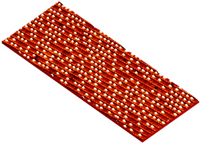
Atomic wires on a silicon surface. An array of "tracks," each only 5 atoms wide, is self-assembled with atomic precision on a stepped silicon surface. Nearby atomic steps are not visible in this image, but their presence forces all the tracks to align along the same direction. This particular surface reconstruction is called Si(111)5×2-Au, which means that it is induced by gold atoms and the structure is periodic (2 atoms along and 5 atoms across the tracks). Note that the gold atoms themselves are not visible on this STM image. The large bright protrusions are silicon atoms, so are the atomic chains that decorate the edge of each track.
Atomic Memory
In his famous 1959 There's Plenty of Room at the Bottom talk, Richard Feynman challenged physicists to consider whether it would be possible to create devices at the level of individual atoms. One of these challenges was creating a memory with the ultimate storage density, that is storing 1 bit of information in 1 atom. Feynman predicted that a cube 5 atoms on each side would be the practical limit for the size of 1 bit, because at a closer spacing the adjacent atomic bits will have too high a probability of affecting each other. The self-assembled silicon atomic memory is a perfect system to test this storage density limit.

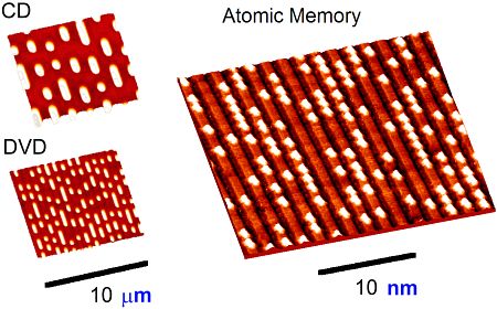
Atomic memory on a silicon surface. The silicon atoms that appear as bright protrusions along the self-assembled tracks can be used to store information in a way similar to that used to record information on CD-ROMs and DVD-ROMs. In this atomic memory, the presence or absence of an atom in a predefined position along the track indicates 1 or 0, respectively. These tracks are only 5 atoms wide, which is approximately 1000 times narrower than tracks on a CD-ROM. Accordingly, the storage density of this atomic memory is 1,000,000 times higher than that of a CD-ROM.
Franz Himpsel's atomic memory page describes the actual reading and writing procedure for this atomic memory. Briefly, first silicon atoms can be evaporated onto the surface to completely fill the tracks with bright protrusions (this experiment incidentally confirmed that protrusions are silicon rather than gold atoms). This initial state can be thought of as reformatting a hard drive to switch all the bits to 1. To write information, atoms can be selectively removed from the track using voltage pulses from an atomically sharp STM tip, as shown in this sequence of STM images. The same STM tip can then be used to read the recorded information.
Because this atomic memory is based on a self-assembled structure of a silicon surface, the atomic positions remain precise even at room temperature—an effect impossible to achieve on metal surfaces, where most of the atomic manipulation has been traditionally done. Somewhat surprisingly, the readout speed using an STM is faster than the speed of DNA replication, even though the two systems have comparable storage densities: 20 atoms/bit for silicon atomic memory vs. 32 atoms/bit for DNA.
selected media coverage
BBC News, UW-Madison, IoP, New Scientist, EE Times, TRN, Slashdot.
Atomic Wires
Can atomic chains on silicon surfaces, such as those seen on the top figure on this page, be considered atomic wires? One actually has to start by asking how a true atomic wire can really be measured—even an atomically sharp STM tip can be too coarse of a probe for such a delicate task.
Photoelectron spectroscopy (PES) to the rescue. In a PES experiment, for a prototype of which Einstein won his Nobel Prize, a beam of energetic light (UV and higher energies) illuminates a sample and ejects electrons (which are called photoelectrons) from the surface.

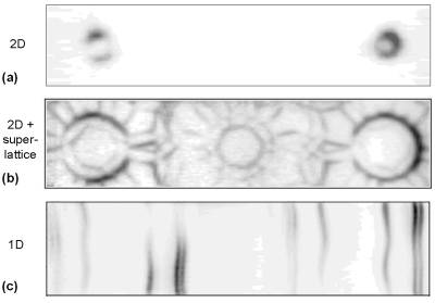
2D and 1D electronic structures on silicon surfaces observed using photoelectron spectroscopy.
(a) 2D electrons on Si(111)√3×√3-Ag;
(b) Si(111)√3×√3-Ag with a superlattice of Au atoms;
(c) nearly-1D electrons on Si(553)-Au.
With sophisticated modern detectors, it is possible to measure a complete set of characteristics (quantum numbers) of photoelectrons, and thus to reconstruct how they were moving before they were ejected from the sample. And since the motion of electrons is what makes a conducting wire, the telltale signatures of a low-dimensional (2D and 1D) conductors can be deduced from the photoelectron spectra. For example, in the above figure, circles indicate 2D electrons, and straight lines—1D ones. The nearly-straight lines observed for atomic chains on Si(553)-Au surface, which has a structure similar to Si(111)5×2-Au shown above, indicate that these chains indeed act as one-dimensional wires. In other words, even though the surface itself is two-dimensional, the conducting electrons are actually only hopping along and not across the atomic chains, which effectively makes the electrons one-dimensional and also means that these atomic chains are acting as the narrowest wires that can be physically made.
Atomically-perfect Templates
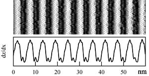
Among the many characteristics that make silicon surfaces excellent nanoscale templates, is their ability to self-organize into atomically perfect templates. The silicon grating structure shown below represents a limiting case of structural perfection for a particular class of stepped silicon surfaces. For this surface the angle at which the wafer was cut matches exactly the slope produced by an array of the narrowest stable atomic terraces separated by atomic steps. Because both steps and terraces have a specific stable structure, the perfect periodicity is maintained along the steps, as can be seen on the averaged cross-sectional profile.

Atomically accurate silicon grating. A series of atomic steps with the perfect periodicity of 17 atomic rows (5.73 nm) for Si(557). STM image of the atomic steps and terraces and a cross-sectional profile averaged along the y axis.
References
- Atomic Scale Memory at a Silicon Surface (230 kB), Nanotechnology 13, 499 (2002).
- Atomic Memory description by Franz Himpsel.
- Electronic Structure of Atomic Chains on Vicinal Si(111)-Au (760 kB), Phys. Rev. B 64, 035406 (2001).
- Atomically Accurate Si Grating with 5.73 nm Period (360 kB), Appl. Phys. Lett. 79, 1608 (2001).